‘I-Cube4’ incorporates four HBMs and one logic die on a paper-thin silicon interposer, supporting enhanced thermal management as well as stable power supply
SEOUL, South Korea–(BUSINESS WIRE)–Samsung Electronics Co., Ltd., a world leader in advanced semiconductor technology, today announced the immediate availability of its next-generation 2.5D packaging technology Interposer-Cube4 (I-Cube4), leading the evolution of chip packaging technology once again.
![]()
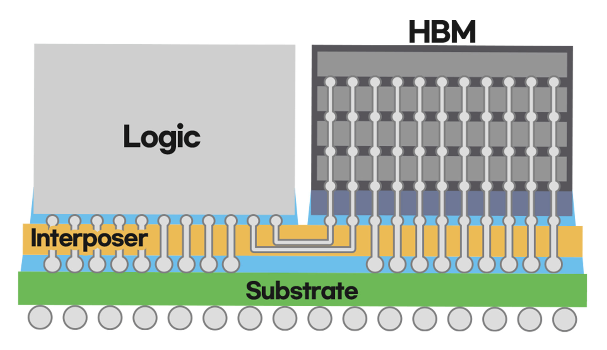
Samsung’s I-CubeTM is a heterogeneous integration technology that horizontally places one or more logic dies (CPU, GPU, etc.) and several High Bandwidth Memory (HBM) dies on top of a silicon interposer, making multiple dies operate as a single chip in one package.
Samsung’s new I-Cube4, which incorporates four HBMs and one logic die, was developed in March as the successor of I-Cube2. From high-performance computing (HPC) to AI, 5G, cloud and large data center applications, I-Cube4 is expected to bring another level of fast communication and power efficiency between logic and memory through heterogeneous integration.
“With the explosion of high-performance applications, it is essential to provide a total foundry solution with heterogeneous integration technology to improve the overall performance and power efficiency of chips,” said Moonsoo Kang, senior vice president of Foundry Market Strategy at Samsung Electronics. “With the mass-production experience amassed through I-Cube2 and the commercial breakthroughs of I-Cube4, Samsung will wholly support customers’ product implementations.”
In general, the silicon interposer area proportionally increases to accommodate more logic dies and HBMs. Since the silicon interposer in the I-Cube is thinner (around 100? thick) than paper, the chances of bending or warping a larger interposer becomes higher, which negatively impacts product quality.
With strong expertise and knowledge on semiconductors, Samsung has studied how to control interposer warpage and thermal expansion through changes to material and thickness, succeeding in commercializing the I-Cube4 solution.
Additionally, Samsung has developed its own mold-free structure for I-Cube4 to efficiently remove heat and enhanced its yield by conducting a pre-screening test that can filter out defective products during the fabrication process. This approach provides additional benefits such as a reduction in the number of process steps, which result in cost savings and shorter turnaround time.
Since the launch of I-Cube2 in 2018 and eXtended-Cube (X-Cube) in 2020, Samsung’s heterogeneous integration technology has signaled a new era in the high-performance computing market. Samsung is currently developing more advanced packaging technologies to I-Cube6 and higher by using a combination of advanced process nodes, high speed interface IPs and advanced 2.5/3D packaging technologies, which will help customers design their products in the most effective way.
About Samsung Electronics Co., Ltd.
Samsung inspires the world and shapes the future with transformative ideas and technologies. The company is redefining the worlds of TVs, smartphones, wearable devices, tablets, digital appliances, network systems, and memory, system LSI, foundry and LED solutions. For the latest news, please visit the Samsung Newsroom at http://news.samsung.com.

Contacts
Clara (Eunyul) Lee
Samsung Electronics, Co., Ltd.
[email protected]